Xilinx Decimal Counter
CS 240
50 points, due May 10, 2010
In this assignment you'll be implementing a decimal up/down counter in VHDL
and using the Xilinx boards to test your design.
- 100 MHz clock. The clock signal arrives at the FPGA on pin P88.
- !Reset. The reset signal arrives at the FPGA on pin P50 (The D0 pin
of the parallel port).
- Hold. The hold signal arrives at the FPGA on pin P48 (The D1 pin of
the parallel port).
- Up/!Down. The up/!down signal arrives at the FPGA on pin P42 (The D2
pin of the parallel port).
- Output a logic '1' on P41. This will disable the FLASH from driving
the data bus it shares with the seven segment display.
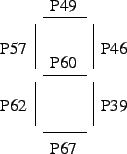
- This figure shows the mapping between seven segment display segments
and FPGA pins:
- When !reset is brought low, the count should reset to 0. This signal
has highest priority.
- When hold is brought high, the current count should be held.
- When hold is low and up/!down is high the counter counts up. When
hold is low and up/!down is low the counter counts down.
Only a decimal (digits 0-9) count should be displayed. The counter should
count modulo 10.
- The count frequency should be about 1 Hz.
- The hold and up/!down inputs are to be synchronized at approximately
a 10 Hz rate.
- Clock signals are to be buffered through BUFG components.
- All clocks should be nominal square waves.
Refer to the Design Notes section for explanation of the diagram.
- Each unique component shown in the block diagram should be designed
as an individual VHDL entity using dataflow or behavioral VHDL. (Except
for the components already provided, such as IBUF and BUFG.) Your
top-level VHDL entity should, using structural VHDL, instantiate all
needed components and connect them using signals.
- Noting the following will save you from a major headache: the
library and use statements must appear before each entity
declaration, not just once at the top of the VHDL file.
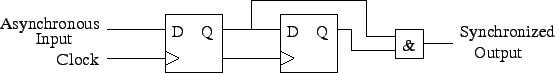
- Here is the schematic drawing for a synchronizer:
- ``Frequency divider'' is a fancy term for ``counter.''
A test driver program will be available on the course home page.
Executable and source code will both be available.
E-mail a copy of your commented VHDL source code and your .bit
file to kelliher[at]goucher.edu.
Thomas P. Kelliher
2010-04-26
Tom Kelliher
![\includegraphics[width=6.5in]{Figures/block.eps}](hw07img2.png)