NAND, Two-Level Implementations, Parity
Tom Kelliher, CS 240
Feb. 8, 2010
Collect homework assignments.
Read 2.9, 6.1-6.2.
New homework assignment.
Simplifying K-maps.
- NAND gates.
- Two-level physical realizations.
- Parity generation and checking.
- BCD to 7-segment decoder example.
Circuit technologies.
- Not AND. Symbol. Truth table.
- At the physical level, this is what we work with.
- Completeness: Given a two-input NAND show how to implement inverter,
AND, OR.
- NOR completely analogous.
Given that we only have NAND gates, implement:
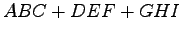 . (Draw
using AND and OR, derive NAND implementation, and draw.)
. (Draw
using AND and OR, derive NAND implementation, and draw.)
- EXOR symbol, truth table.
- EXOR = odd function. (NEXOR = even)
- A ``big'' EXOR can be recursively constructed from ``small'' EXORs.
- Parity generate and check circuit for ASCII data:
Show a few examples.
Simplify and implement  .
.
Thomas P. Kelliher
2010-02-05
Tom Kelliher
![\begin{figure}\centering\includegraphics[]{Figures/parity.eps}\end{figure}](feb08img2.png)