Memory: ROM and RAM

Tom Kelliher, CS 220

May 5, 2008

Administrivia

Announcements

Homework due Wednesday!

Assignment

Look over Chapter 8.

From Last Time

Counters

Outline

  1. Introduction.

  2. ROM, FLASH.

  3. RAM.

Coming Up

Details on RAM.

Introduction

  1. What is memory?

  2. Volatile vs. non-volatile.

  3. RAM characteristics: speed, density, power.

  4. Memory hierarchy: registers, cache, main memory, etc.

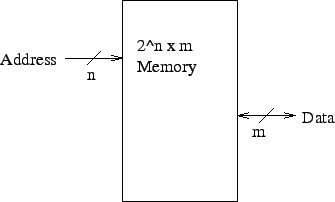
  5. General structure:

    \includegraphics{Figures/memory.eps}

ROM

  1. Technologies: PROM, EPROM (UV), EEPROM, EAPROM, FLASH.

  2. Where do you find ROM in a PC?

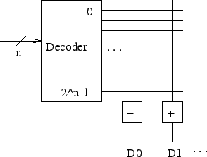
  3. Structure of a ROM:

    \includegraphics{Figures/rom.eps}

    Minterms, fusible links.

  4. Usage: program storage, generation of combinational functions.

    How do you use for combinational functions?

FLASH

  1. A specific type of EEPROM.

  2. Erasure sets all the bits (to 1).

    Programming/writing resets a bit (to 0).

  3. Two types:
    1. NOR:
      1. Cells connected in parallel to bit lines. Allows random access.

        Similar to pull-down plane in a NOR gate, hence the name.

        \includegraphics[width=4in]{Figures/norLayout.eps}

      2. Long erase and write times.

      3. Allows random access to any memory location.

        ``Drop-in'' replacement for ROM (system BIOS, other firmware).

      4. Sustains $10^5$ erase cycles.

    2. NAND:
      1. Cells connected in series to bit lines. Prohibits random access.

      2. Faster erase and write times. Denser.

      3. Block-oriented access. Suitable for secondary storage.

        Block may consist of 64 pages of 2 KB each. Writes can be done on a per page basis; erases on a per block basis.

      4. Sustains $10^6$ erase cycles.

  4. Programming NOR FLASH

    \includegraphics[width=3in]{Figures/flashProgramming.eps}

    1. Cell resembles standard MOSFET, but there is a second, insulated gate -- the ``floating gate,'' which is completely insulated by the oxide layer.

    2. To program, an elevated voltage is applied to gate and drain. Channel conducts.

    3. Elevated voltage created by a charge pump.

    4. Source/drain current high enough to allow some high-energy electrons to jump to the FG, charging it. This charge is essentially permanent.

    5. Charge on FG modifies the threshold voltage, essentially forcing the transistor into an always open state (non-conducting), storing a 0.

  5. Erasing NOR FLASH

    \includegraphics[width=3in]{Figures/flashErase.eps}

    1. Apply large negative voltage from drain to gate.

    2. Electrons on FG are pulled to drain via quantum tunnelling.

    3. Threshold voltage restored, allowing transistor to once again conduct, storing a 1.

    4. Cells are erased in blocks.

  6. Memory wear, bad block detection and management, wear levelling.

    Remap blocks around bad spots, or to level erasure effects. (Per block erasure counters needed).

    Checksums used to detect and correct block failures.

RAM

  1. Additional inputs: !Enable, Read/!Write

  2. Static RAM: latches, inverter pair.

    Used for caches. Fast. Not dense. High power.

  3. Dynamic RAM: stored charge on a capacitor.
    1. Leakage, refresh.

    2. Used for main memory. Slow. Dense. Low power.

    3. Sizes. I/O pin limitations. Solutions: one bit wide, address multiplexing. 2-D structure.

    4. Additional inputs: RAS, CAS.

  4. Read/Write sequences.

    Write strobe with respect to the clock signal. Importance of address bus settling before write asserts.


Thomas P. Kelliher 2008-04-30
Tom Kelliher