Voltage, current, power, speed.
Delay may be asymmetric:  ,
,  . Max of both:
  .
.
Tom Kelliher, CS 220
Sept. 24, 2003
Read 3.1--3.
NAND gates, two-level implementation, parity.
Combinational logic design process and simulation.
Voltage, current, power, speed.
Delay may be asymmetric: , . Max of both: .
An electronic switch:
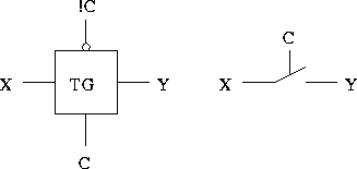
Typically used to enable writes onto a bus. For examples, two CPUs sharing a memory bus. Bus arbitration.
Can be used in more crafty ways: viewing an EXOR as a ``conditional inverter:''
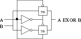
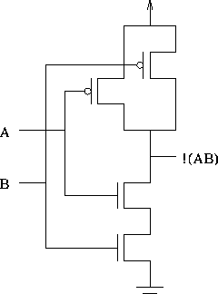
Eight transistors; two gate delays.
The standard NAND implementation requires four gates (16 transistors) and has a propagation delay of three gate delays.
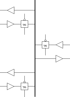
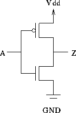
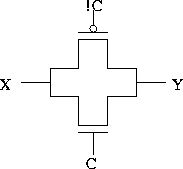
Diagrams:
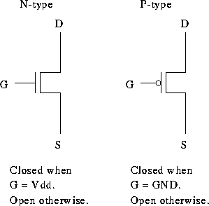
A CMOS inverter:
A CMOS transmission gate:
A CMOS 2-input NAND gate:
What determines power dissipation? Switching frequency.
Why transport delay isn't a good model: It takes time to move the charge on the gate. This is correctly modeled with inertial delay.