Sequential Logic Circuits
Tom Kelliher, CS26
Oct. 10, 1996
Reading:
- Study: A.6--A.10.
- Glance at: A.11--A.12.
To summarize combinational design, we'll do one or two of the following.
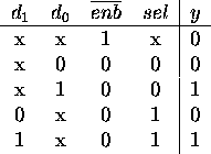
- Design and implement a 2-1 multiplexer, using a K-map for
minimization of the output equation. Here's the truth table:
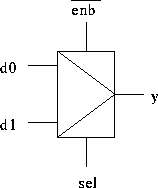
A multiplexer works like a switch. One way of drawing them is:
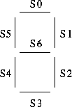
- Design and implement a circuit to take a BCD-encoded digit and drive
a seven-segment display (used in watches and calculators). Use a K-map to
minimize each of the seven output equations. Take advantage of don't
cares. Here is the labeling for the display:
- Design and implement a circuit to take a BCD-encoded digit and
increment it by one (nine should be ``incremented'' to zero). Use a K-map
to minimize each of the four output equations. Take advantage of don't
cares.
- Sequential circuits.
- Combinational circuits have no memory.
- Memory provided by feedback --- output becomes input in an
``earlier'' part of the circuit.
- Clock signal --- a special control signal used to orchestrate
state changes within the circuit. Types of clocked circuits:
- Level sensitive --- state changes may occur when the clock signal
is at a particular level (0 or 1).
- Master-Slave --- The use of two clock signals with pairs of
level-sensitive flip-flops to prevent ``double-clocking.'' Suffers from
``ones-catching.''
- Edge-triggered --- state changes may occur only on a clock
transition (edge).
- State --- The values stored by sequential circuit elements
(flip-flops, latches). The value of a particular signal.
Types of flip-flops:
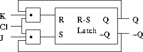
- R-S. Unclocked R-S:
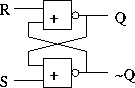
Truth table:
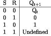
Inputs always sampled --- state changes at any time.
Timing diagram?
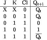
- J-K. Clocked (level-sensitive) J-K:
Truth table:
Timing diagram?
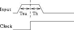
Important timing nomenclature:
- Propagation delay.
- Set-up time.
- Hold time.
Master-slave J-K:
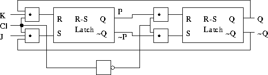
Timing diagram?
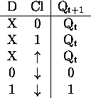
- D. Negative edge-triggered D flip-flop:
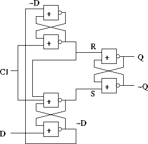
Truth table:
How does it work? Consider:
- Clock high.
- Falling edge (inputs to 2nd stage latched).
- Clock low.
- Rising edge.
- Multiplexer ---
 -to-1 switch:
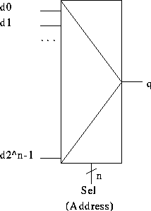
``Tiling'' multiple multiplexers to switch words.
- Decoder --- 1-of-
 driver:
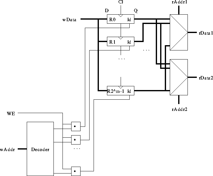
- Tiling D flip-flops.
- Selective loading.
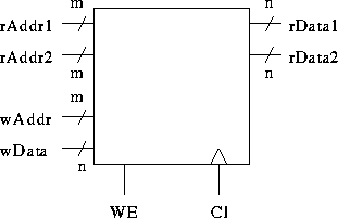
The MIPS statement
add $t0, $t1, $t2
must read two operands and write one in a single cycle.
Need a three-port register file.
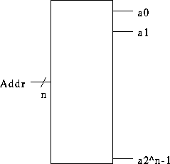
General block diagram of register file:
Detailed block diagram:
Thomas P. Kelliher
Wed Oct 9 15:12:30 EDT 1996
Tom Kelliher