Tom Kelliher, CS 220
Nov. 7, 1997
Read Chapter 7. Homework assignment due Nov. 14, available on class home page.
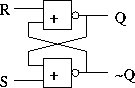
An RS latch:
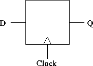
A D flip-flop:
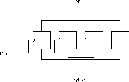
A four-bit register:
Block diagram of a register file:
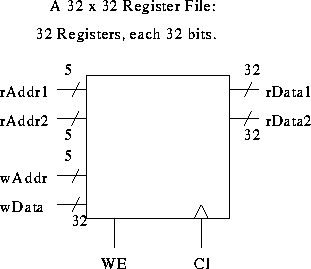
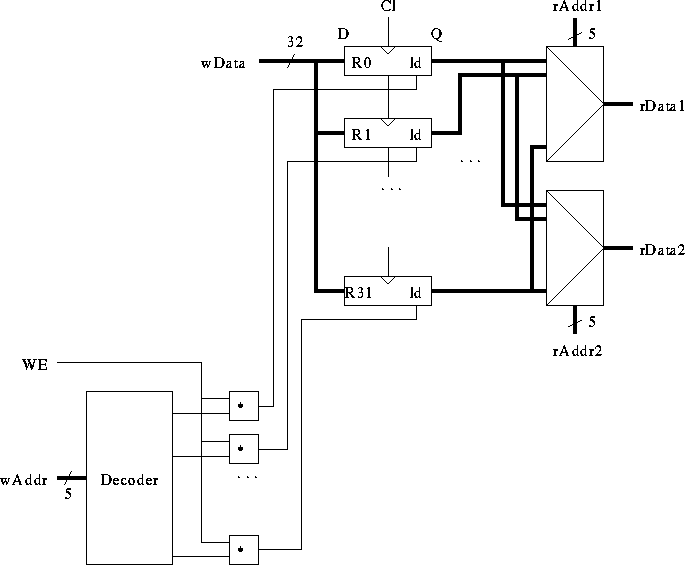
More detail of the register file:
 outputs. The inputs, interpreted as a
binary number, specify which one of the output lines to drive high
(logic 1). All other output lines stay low (logic 0).
outputs. The inputs, interpreted as a
binary number, specify which one of the output lines to drive high
(logic 1). All other output lines stay low (logic 0).
 -to-1 switch. The n address inputs specifies which
of the
-to-1 switch. The n address inputs specifies which
of the  data inputs to send to the output. To switch 32 32-bit lines,
32 32-to-1 muxes are used, with their address inputs all tied together.
(Demonstrate switching 4 4-bit registers.)
data inputs to send to the output. To switch 32 32-bit lines,
32 32-to-1 muxes are used, with their address inputs all tied together.
(Demonstrate switching 4 4-bit registers.)
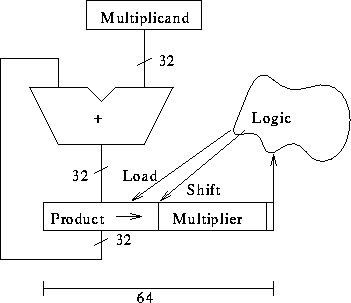
Block diagram:
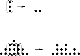
Consider the partial product matrix for four-bit multiplication:

Consider the effects of carry-save adders:
Continue this. How many levels?
But, this differs from:
Tradeoff: minimize number of CSAs or minimize time.
Tradeoff: speed of Wallace tree vs. speed of shift accumulate.
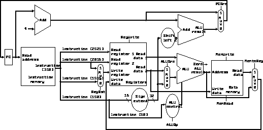
A model of a simple, non-pipelined datapath:
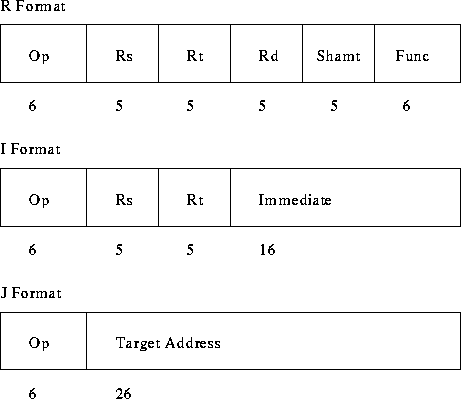
The MIPS instruction formats:
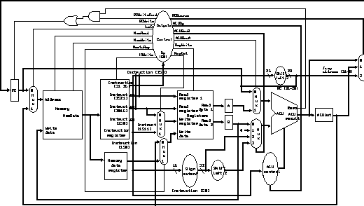
Walk through: