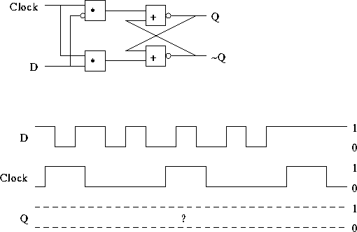


The waveform is applied to the inputs of the circuit, with time represented on the horizontal axis. The vertical axis represents the logical values 0 and 1, as indicated. Copy the waveforms to another sheet, and complete Q's waveform.
CS 220
40 points, due Nov. 14, 1997


The waveform is applied to the inputs of the circuit, with time represented on the horizontal axis. The vertical axis represents the logical values 0 and 1, as indicated. Copy the waveforms to another sheet, and complete Q's waveform.