- Assume that a memory operation takes the same amount of time as
one internal CPU step. Rewrite the control sequence.
 1: PCout, MARin, Read, Clear Y, Set carry-in to ALU, Add, Zin
 2: Zout, PCin, MDRmemin
 3: MDRbusout, IRin
 4: R3out, MARin, Read
 5: R1out, Yin, MDRmemin
 6: MDRbusout, Add, Zin
 7: Zout, R1in, End
- Assume that a memory operation takes the same amount of time as
two internal CPU steps. Rewrite the control sequence.
 1: PCout, MARin, Read, Clear Y, Set carry-in to ALU, Add, Zin
 2: Zout, PCin
 3: MDRmemin
 4: MDRbusout, IRin
 5: R3out, MARin, Read
 6: R1out, Yin            # These could be carried out in the next step.
 7: MDRmemin
 8: MDRbusout, Add, Zin
 9: Zout, R1in, End

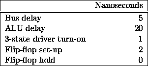
What is the minimum time that must be allowed for performing each of the following operations?
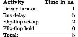
- Transfer data from one register to another.

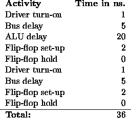
- Increment the program counter.

Next, consider the Add instruction that has the control sequence given in Figure 3.5. The CPU is driven by a continuously running clock signal, such that each control step is 20 ns. in duration. How long will the CPU have to wait in steps 2 and 5, assuming that a memory read operation takes 80 ns. to complete? What percentage of the time is the CPU idle during execution of this instruction?
The CPU waits for 60 ns. in each of the steps. (It spends 20 ns. working in each of the steps.) The total execution time of the instruction is 260 ns. with 120 ns. of waiting. The CPU is idle for 46% of the instruction's execution time.
- Add the immediate value NUM to register R1.
- Add the contents of memory location NUM (direct addressing) to
register R1.
- Add the immediate value NUM to register R1 (indexed addressing);
fetch the memory location whose address is that sum and add it to
register R2.
Write the sequence of control steps for:
- The bus structure in Figure 3.1.
- Add the immediate value NUM to register R1.
 1: PCout, MARin, Read, Clear Y, Set carry-in to ALU, Add, Zin
 2: Zout, PCin, WMFC
 3: MDRout, IRin
 4: PCout, MARin, Read, Clear Y, Set carry-in to ALU, Add, Zin
 5: Zout, PCin
 6: R1out, Yin, WMFC
 7: MDRout, Add, Zin
 8: Zout, R1in, End
- Add the contents of memory location NUM (direct addressing) to
register R1.
 1: PCout, MARin, Read, Clear Y, Set carry-in to ALU, Add, Zin
 2: Zout, PCin, WMFC
 3: MDRout, IRin
 4: PCout, MARin, Read, Clear Y, Set carry-in to ALU, Add, Zin
 5: Zout, PCin
 6: R1out, Yin, WMFC
 7: MDRout, MARin, Read, WMFC
 8: MDRout, Add, Zin
 9: Zout, R1in, End
- Add the immediate value NUM to register R1 (indexed addressing);
fetch the memory location whose address is that sum and add it to
register R2.
 1: PCout, MARin, Read, Clear Y, Set carry-in to ALU, Add, Zin
 2: Zout, PCin, WMFC
 3: MDRout, IRin
 4: PCout, MARin, Read, Clear Y, Set carry-in to ALU, Add, Zin
 5: Zout, PCin
 6: R1out, Yin, WMFC
 7: MDRout, Add, Zin
 8: Zout, MARin, Read
 9: R2out, Yin, WMFC
10: MDRout, Add, Zin
11: Zout, R2in, End
- Add the immediate value NUM to register R1.
- The bus structure in Figure 3.13.
- Add the immediate value NUM to register R1.
 1: PCoutA, Pass A, MARin, Read
 2: PCoutA, Clear B, Set carry-in to ALU, Add, PCin, WMFC
 3: MDRoutB, IRin
 4: PCoutA, Pass A, MARin, Read
 5: PCoutA, Clear B, Set carry-in to ALU, Add, PCin, WMFC
 6: R1outA, MDRoutB, Add, R1in, End
- Add the contents of memory location NUM (direct addressing) to
register R1.
 1: PCoutA, Pass A, MARin, Read
 2: PCoutA, Clear B, Set carry-in to ALU, Add, PCin, WMFC
 3: MDRoutB, IRin
 4: PCoutA, Pass A, MARin, Read
 5: PCoutA, Clear B, Set carry-in to ALU, Add, PCin, WMFC
 6: MDRoutA, Pass A, MARin, Read, WMFC
 7: R1outA, MDRoutB, Add, R1in, End
- Add the immediate value NUM to register R1 (indexed addressing);
fetch the memory location whose address is that sum and add it to
register R2.
 1: PCoutA, Pass A, MARin, Read
 2: PCoutA, Clear B, Set carry-in to ALU, Add, PCin, WMFC
 3: MDRoutB, IRin
 4: PCoutA, Pass A, MARin, Read
 5: PCoutA, Clear B, Set carry-in to ALU, Add, PCin, WMFC
 6: R1outA, MDRoutB, Add, MARin, Read, WMFC
 7: R2outA, MDRoutB, Add, R2in, End
- Add the immediate value NUM to register R1.
- Add (R3), R1, Figure 3.5.
 1: PCoutA, Pass A, MARin, Read
 2: PCoutA, Clear B, Set carry-in to ALU, Add, PCin, WMFC
 3: MDRoutB, IRin
 4: R3outA, Pass A, MARin, Read, WMFC
 5: R1outA, MDRoutB, Add, R1in, End
- The branch-on-negative instruction discussed in Section 3.2.1.
 1: PCoutA, Pass A, MARin, Read
 2: PCoutA, Clear B, Set carry-in to ALU, Add, PCin, WMFC
 3: MDRoutB, IRin
 4: If N = 0 then End
 5: Offset-field-of-IRout, PCoutB, Add, PCin, End
- jal
 1: PCoutA, Pass A, MARin, Read
 2: PCoutA, Clear B, Set carry-in to ALU, Add, PCin, WMFC
 3: MDRoutB, IRin
 4: PCoutA, Pass A, R31in
 5: Branch-target-field-of-IRout, Pass A, PCin, End
- jr
 1: PCoutA, Pass A, MARin, Read
 2: PCoutA, Clear B, Set carry-in to ALU, Add, PCin, WMFC
 3: MDRoutB, IRin
 4: R31outA, Pass A, PCin, End